
Are you unsure of where to begin when it comes to your FPGA designs?
The term FPGA can be confusing if you are not already familiar with the semiconductor industry. An FPGA is like a large collection of lego building blocks, in which you can construct anything imaginable through complex programming. These manufactured lego-blocks are also known as Lookup Tables (LUTs) and Flip-Flops (FF).
Moving forward with manufacturing, we are reliant on the target FPGA family and their vendors. You may notice that the lego-blocks LUTs and/or FF are fixed. This simply refers to the limited resources existing within each target FPGA.
Let’s dive in deeper to give you a more accurate and clear understanding of how FPGAs work.
Why are Lookup Tables (LUTs) and Flip-Flops (FF) important?
LUTs and FF are the fundamental basis of any FPGA. Some of the basic functions of Lookup Tables and Flip Flops include calculating any mathematical computation or registers that hold these computed values.
More specifically, a Lookup Table is in fact, a table that holds the data relevant to your FPGA design as it is customized to your needs and instructions.
Flip-flops are binary registers that work between clock cycles. So, on every clock cycle a FF registers the data and holds it until the next cycle.
Where can we find these LUTs and FF?
We can understand this by noting that FPGA resources are a collection of limited Slices, which are known as Configurable Logic Blocks (CLB). LUTs, flip-flops are placed inside each Slice.
FPGA Fabrics Contain The Following Elements:
- Block Rams (Bram’s)
- Distributed Rams
- Digital Signal Processing (DSP’s) blocks
- PCIe blocks
- GTP blocks (Gigabit Transceivers)
- Xilinx Analog to Digital Conversion (XADC)
- Clock Management Blocks
- User Input/Output (i/o) Pins.
These resources will function as building blocks to allow you the best optimizations of your customized projects.
How can we calculate LUTs and FF?
In this blog post, we’ll use the Arty A7-35T as an example: (https://digilent.com/shop/arty-a7-artix-7-fpga-development-board/).
If we take a look at the Development Board above, our target FPGA is at XC7A35T, which is highlighted.
Here, there are 5,200 Slices. Each Slice contains 4 LUTs and 8 Flip-flops. Only some slices can use their LUTs as distributed RAM or SRLs.
So now, we just have to multiply the number of Slices times the number of LUTs or FF: 5,200 x 4 = 20,800 LUTs 5,200 x 8 = 41,600 FF
For a better understanding, the FPGA fabric in this example has some special abilities. We can see that most Logic User Applications will fit inside this individual fabric, with an additional number of DSP, BRAM/Distributed Ram and PCIE blocks.
Diving Deeper Into LUTs
There are 5 types of LUTs that you can use in your FPGA:
- LUT2 (two input, 1 output LUT)
- LUT3 (three input, 1 output LUT)
- LUT4 (four input, 1 output LUT)
- LUT5 (five input, 1 output LUT)
- LUT6 (six input, 1 output LUT)
Here are some sample codes for each type. These are purely combinational designs without any registers or FF (Flip-flops).
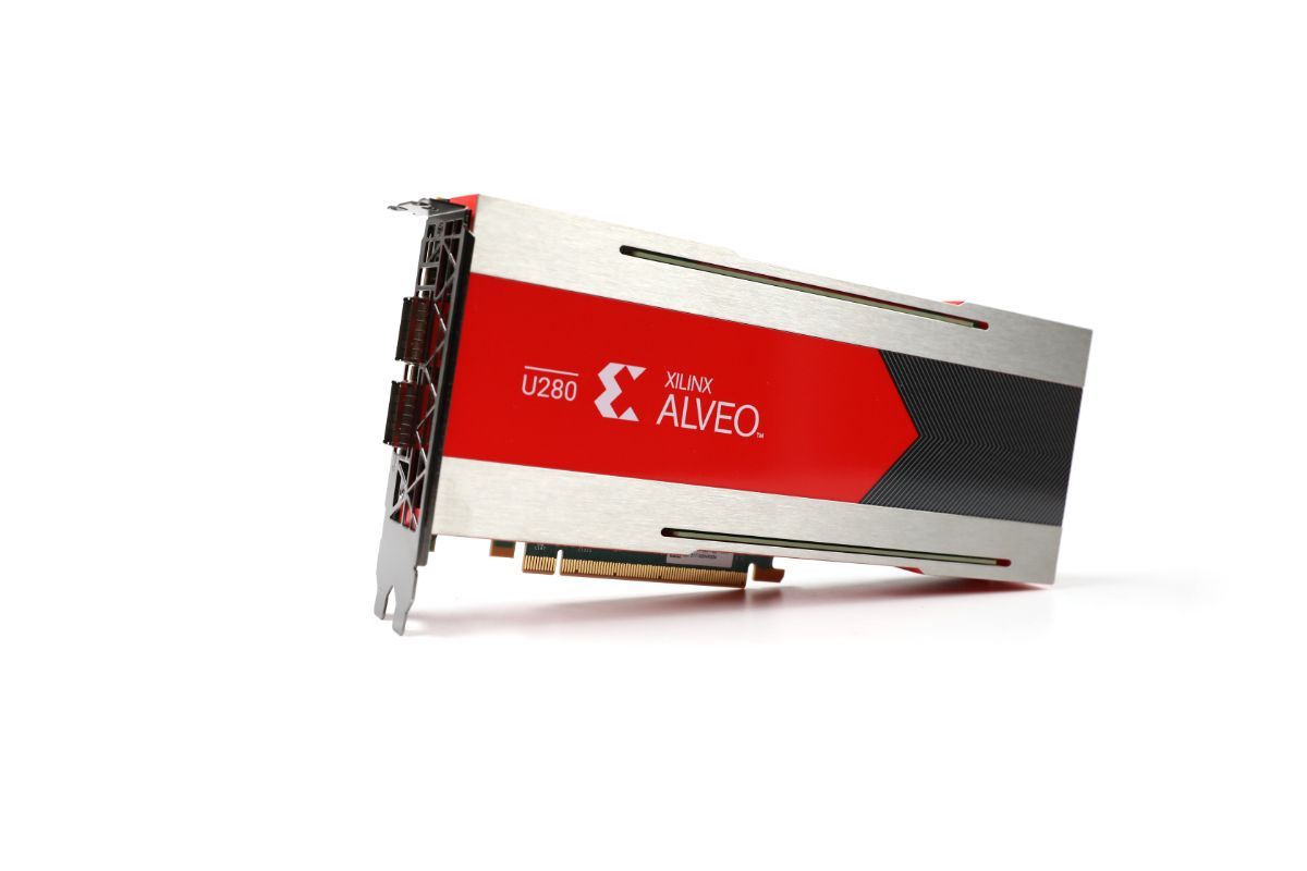
- LUT2:
This is an example of 2-input LUT performing bitwise-xor and generating output c_out.
module lut2(

input wire a_in,

input wire b_in,

output wire c_out

);

assign c_out = a_in ^ b_in;

endmodule
Post-Synthesis schematic capture using Vivado of LUT2
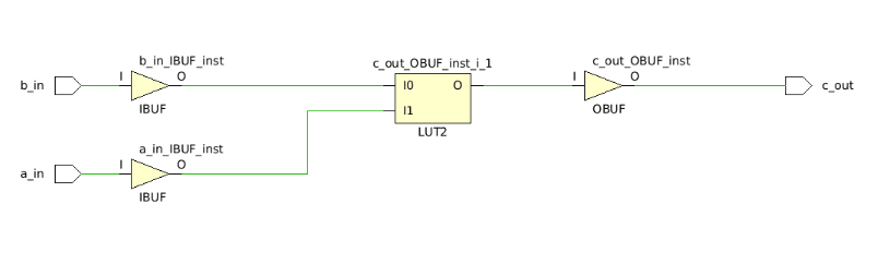
- LUT3:
This is an example of 3-input LUT performing bitwise-and and generating output d_out.
module lut3(

     input wire a_in,

     input wire b_in,

     input wire c_in,

     output wire d_out

 );

 assign d_out = a_in & b_in & c_in;

Endmodule
Post-Synthesis schematic capture using Vivado of LUT3
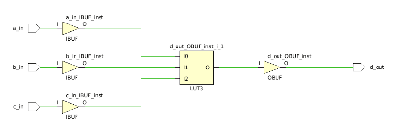
- LUT4:
This is an example of 4-input LUT performing bitwise-or and generating output e_out.
module lut4(

     input wire a_in,

     input wire b_in,

     input wire c_in,

     input wire d_in,

     output wire e_out

  );

  assign e_out = a_in | b_in | c_in | d_in ;

  endmodule
Post-Synthesis schematic capture using Vivado of LUT4
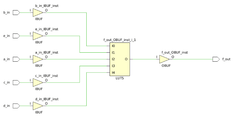
- LUT5:
This is an example of 5-input LUT performing bitwise-xor and generating output f_out.
  module lut5(

       input wire a_in,

       input wire b_in,

       input wire c_in,

       input wire d_in,

       input wire e_in,

       output wire f_out

    );

    assign f_out = a_in ^ b_in ^ c_in ^ d_in ^ e_in;

    endmodule
Post-Synthesis schematic capture using Vivado of LUT5
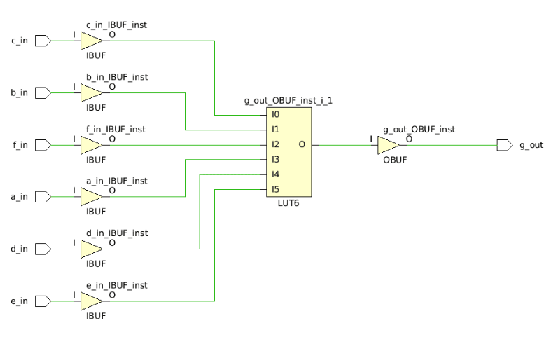
- LUT6
This is an example of 6-input LUT performing bitwise-xor and generating output g_out.
  module lut6(

        input wire a_in,

        input wire b_in,

        input wire c_in,

        input wire d_in,

        input wire e_in,

        input wire f_in,

        output wire g_out

    );

   assign g_out = a_in ^ b_in ^ c_in ^ d_in ^ e_in ^ f_in;

   endmodule
Post-Synthesis schematic capture using Vivado of LUT6
Next, we can make a top_module in which we can instantiate all types of LUTs to show a method of module instantiation in Verilog and all registers in design.
I hope that with this blog post you’ve gained a basic understanding of where to start with your FPGA designs and how FPGAs work.
