
Interface Xilinx XDMA PCIe with DDR3 using MIG-IP on Artix-7 FPGA using Nitefury dev board
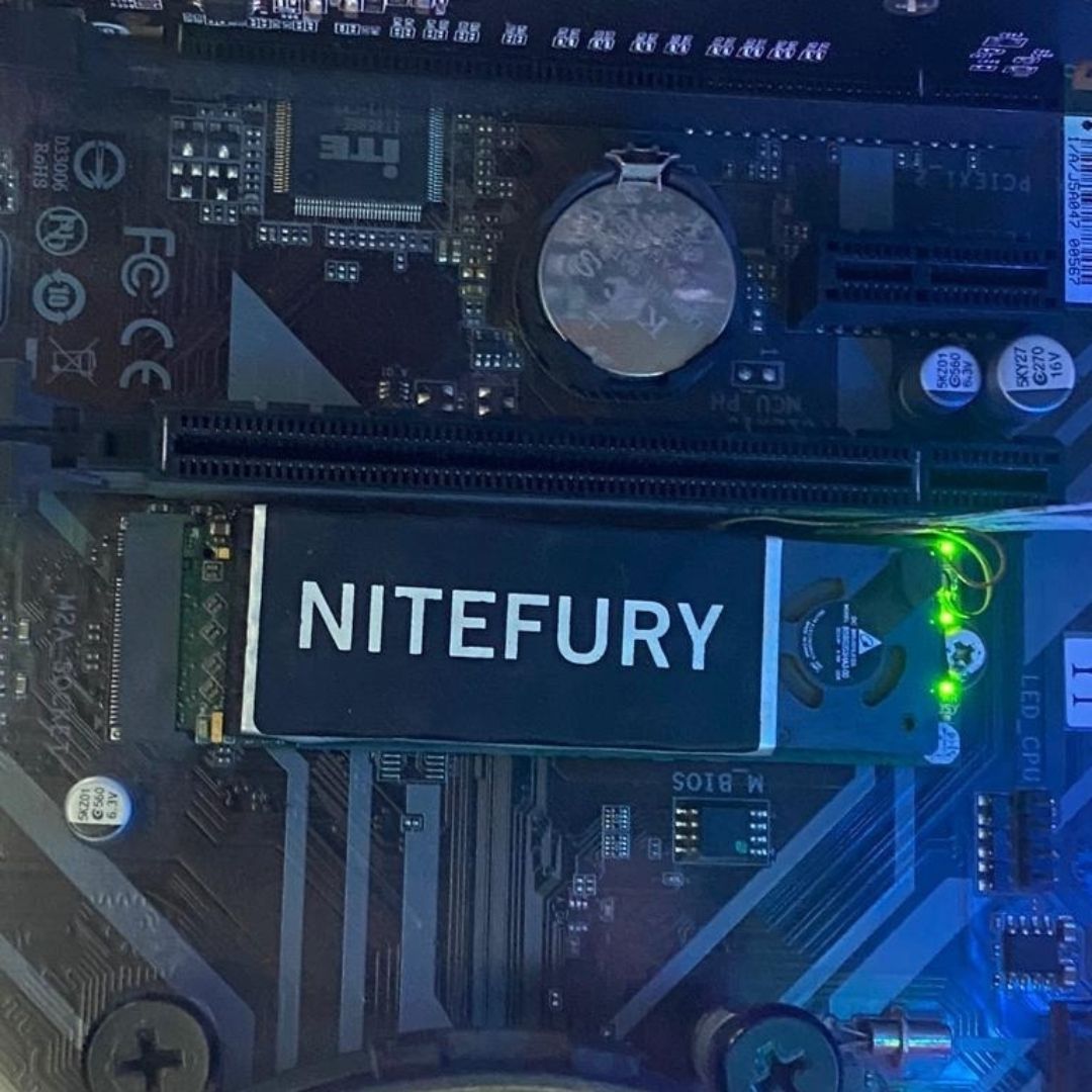
Nitefury is a M.2 form factor FPGA development board that has Artix-7 FPGA with onboard DDR3 memory. It can be connected to a laptop or motherboard that has M.2 pcie connector or that it’s using a M.2 pcie riser.
You can get more info about boards here: https://rhsresearch.com/
What is DMA?
DMA Stands for Direct Memory Access. It’s used to move data from one location in a system to another.
As an example, you could have an ADC (Analog to Digital Converter) generating data, and you can configure DMA to move that generated data to the memory. Why? Well, if you use a microprocessor to do this task, this would make your data-acquisition system too slow. The microprocessor can be used to do other important tasks.
DMA can also be used to read data from the memory to send it to other peripherals such as DAC (Digital to Analog Converter) or to other modules where it can be used for other purposes.
Xilinx provides XDMA PCIe IP to connect the host system with PCIe interface
In this blog post, my goal is to send some data from the host system via PCIe to DDR3 and receive data back from DDR3 memory to the host system.
Here are the steps I followed:
- Set up a Vivado Project
- Configure XDMA PCie IP in Vivado Block Design
- Configure MIG IP for DDR3 memory in Vivado Block Design
- Install XDMA drivers on Host (Linux-System) You can also check the project on GitHub here.
STEP ONE: Setting up Vivado Project
- Once you launch Vivado, Select “Create Project”
- Select “Next”
- Give the project a name, as per your preference
- Give the project a location where you want it to be saved
- Then click on “Next”
- Select “RTL Project”
- Select “Do not specify sources at this time”
- Then select “Next”
- Enter the FPGA part number: - xc7a200tfbg484-3
- Then select “Next” and “Finish”
Once the Vivado project is set up, we can start making block design and start adding and configuring IP.
- On left side of the window, under flow navigator select “Create Block Design”
- Enter a design name then select “OK”
- Click on "add IP" as shown in the picture, and enter XDMA in the search bar.
- Then press "enter" to add IP to block design
STEP TWO: Configuring XDMA PCIe IP
At this point, XDMA IP is not configured, so it needs to be configured as per our requirements.
- In block design select "block automation". It will bring up this window:
- Here the PCIe interface Lane Width is selected to x4 because we have 4 differential lanes on the FPGA dev board. Then select “OK”
- This will create a block design
Next, we have to configure XDMA PCIe IP.
- Double click on “XDMA IP” this will open an IP configuration window
- Set AXI databus to 128-bits.
- This is M_AXI data-width, which will be connected to MIG-IP, which connects to DDR3 memory.
- If you select a 64-bit data bus, the AXI clock frequency will be fixed to 250MHz which may cause timing failure during routing.
- Additionally, we will configure MIG IP with a 128-bit data bus, so Master and Slave both are with the same data bus.
- In PCIe:BARS tab in the image below, select "64bit enable".
- Under PCIe:MISC tab, de-select “configuration management interface” as the image below shows.
- Then select “OK”
Now the XDMA PCIe IP is configured.
STEP THREE: Configuring MIG IP for DDR3 memory
- Add MIG IP in block design as the image below shows.
- Press “enter” to add IP to block design
As seen in the image below, MIG IPis added to block design, but it needs to be configured so it can be connected to XDMA PCIe IP
- Double click on “MIG IP” will start a GUI for MIG configuration.
- Right click on DDR interface of MIG IP as the image below shows, and select “make external”. This port will connect with DDR3 interface between FPGA io pins to DDR3 pins
Now we need to connect M_AXI port of xdma_0 IP in block design with S_AXI of mig_7_series_0 IP.
- M_AXI is a Master AXI bus port
- S_AXI is a Dlave AXI bus port
You can connect M_AXI to S_AXI in 2 possible ways:
- Direct connection
- Using AXI interconnect
Using Direct connection will require making sure that the M_AXI clock freq is the same as S_AXI, as per block design XDMA axi_clock pin is 125MHz and MIG ip ui_clk is 133.33MHz. As these two ports are on different clock frequencies, if you connect this, it will give a block design error. To overcome this problem we use AXI_Interconnect IP.
Using AXI_Interconnect IP helps to connect one or more master AXI ports to multiple slaves. You can also add FIFO buffers in interconnect and connect different clock domains IPs in block design
- Select run connection automation in block design This gui option is to connect XDMA M_AXI port to S_AXI of MIG IP. Vivado will add a new AXI SmartConnect in block design and manage a different clock domain.
- Press “OK”
At this point block design is ready, so now we can make the bitstream.
Before we do, we need to add constraints to our design. These constraints will be required to connect PCIe lanes ports and DDR3 ports. To make it simpler, we have uploaded this project to GitHub.
Making the bitstream
- Under flow navigator on the left side of the window, click on "generate bitstream"
- Once the bitstream is finished generating, we can upload it to FPGA. Make sure to connect USb-JTAG programming cable to FPGA.
- Then open hardware manager. Once the hardware manager is open, then click on "open target"
- Then click on "program device" and give a path to the bitstream file, that will be inside the impl directory of the project. Then click on "program"
STEP FOUR: Installing XDMA drivers
- Download XDMA drivers from the following link: https://github.com/Xilinx/dma_ip_drivers
- Follow the readme document from this link: https://github.com/Xilinx/dma_ip_drivers/blob/master/XDMA/linux-kernel/readme.txt
- Once FPGA is programmed with bitstream, we need to reboot the system with the FPGA board connected to the system. During the reboot, when the system bios boots up, the PCIe device will be enumerated.
- Then we need to run a script load_drivers.sh
- Run this script in terminal with the following command: “Sudo ./load_drivers.sh”
- You can check if FPGA is detected using the following command: “Sudo lspci -vvv -d 10ee:”
- Once the drivers are installed and loaded, its time to write a python script
Additional links for XDMA PCIe
https://www.xilinx.com/video/technology/getting-the-best-performance-with-dma-for-pci-express.html
Feel free to review our core FPGA design services if you need additional assistance.
